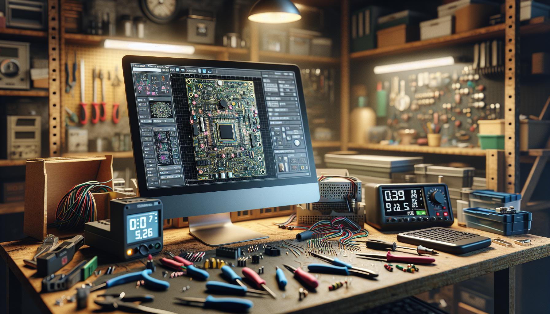
Designing a PCB board for a circuit is a critical step in electronics development that can significantly influence performance and reliability. Whether you’re an experienced engineer or just starting out, understanding the nuances of PCB design can streamline your workflow and help avoid common pitfalls. For those seeking professional assistance or advanced tools, exploring options for PCB design services can simplify the process and enhance results.
Understanding PCB Design Basics
Designing a PCB (Printed Circuit Board) requires knowledge of fundamental concepts that contribute to effective and reliable circuit layouts. Understanding these concepts lays the foundation for creating high-quality PCB designs that meet project specifications.
What Is a PCB?
A PCB is a board that physically supports and connects electronic components. It consists of a non-conductive substrate, typically made of fiberglass or plastic, with conductive pathways etched onto its surface. These pathways, known as traces, allow electrical signals to flow between components such as resistors, capacitors, and integrated circuits. PCB designs facilitate the mechanical and electrical connections, ensuring proper functionality in a wide range of electronic devices.
Types of PCB Designs
PCB designs fall into several categories, each suiting different applications:
- Single-Sided PCBs: These contain components and traces on one side only. This design is cost-effective and ideal for simple electronics, such as basic consumer products.
- Double-Sided PCBs: These feature components on both sides, allowing for more complex circuits. This type uses vias to connect traces between the two sides, accommodating a higher density of components.
- Multilayer PCBs: These are made up of multiple layers of insulation and circuitry, enabling intricate layouts and advanced functionality. They are commonly found in high-performance devices, such as computers and smartphones.
- Flexible PCBs: These boards use flexible materials that can bend or twist. They are suitable for applications where space is limited, such as wearable devices.
- Rigid-Flex PCBs: These combine rigid and flexible sections, allowing for both durability and adaptability. They benefit applications requiring complex designs that need to fit into tight spaces.
Understanding the various types of PCB designs assists in selecting the most suitable approach for specific project requirements.
Essential Tools for PCB Design
Effective PCB design requires specific tools that streamline the process and improve the design’s efficacy. The following subsections detail critical software and simulation tools essential for high-quality PCB design.
PCB Design Software
PCB design software is crucial for creating the layout and schematic of a circuit board. Popular options include:
- Altium Designer: Offers advanced features for high-speed design, extensive libraries, and a user-friendly interface.
- EAGLE: Affordable and accessible for hobbyists, it provides powerful schematic capture and PCB layout capabilities.
- KiCad: A free, open-source tool that supports multi-layer designs and offers an intuitive interface for users.
- OrCAD: Ideal for complex designs, this software provides simulation tools and extensive component libraries.
These tools facilitate efficient design, ensuring precision in connecting electronic components.
Simulation Tools
Simulation tools allow designers to test and validate circuit behavior before manufacturing. Key simulation tools include:
- LTspice: A free simulation software for analog circuits that provides powerful analysis and circuit modeling capabilities.
- Multisim: Combines simulation with a schematic capture tool, allowing comprehensive analysis for both digital and analog circuits.
- Proteus: Integrates both circuit simulation and PCB design, enabling real-time simulation of microcontroller projects.
- PSpice: Offers extensive simulation capabilities, especially suited for mixed-signal designs.
These tools help predict performance issues, saving time and resources during the design phase.
Step-By-Step Guide on How to Design a PCB Board for a Circuit
Designing a PCB board involves several critical steps to ensure a functional and efficient layout. Each step builds on the previous one to create a cohesive and reliable circuit.
Defining the Requirements
Define project requirements clearly before starting the design process. Establish parameters such as the number of components, voltage levels, and thermal considerations. Determine the dimensions of the PCB according to the available space in the final application. Consider environmental factors, such as operating temperature and humidity, that could affect the PCB’s performance. Documenting these specifications creates a solid foundation for the subsequent design stages.
Creating the Schematic
Create a schematic diagram to represent the electrical connections between components. Use PCB design software for accuracy and efficiency. Place all required components on the schematic following the predefined requirements. Connect components using appropriate lines to represent electrical paths, ensuring clarity in the diagram. Confirm the schematic for errors and inconsistencies, as this serves as the blueprint for the PCB layout.
Designing the Layout
Design the PCB layout based on the schematic diagram created earlier. Arrange components on the board according to spatial constraints and ergonomic considerations. Maintain ample space between components to facilitate soldering and heat dissipation. Organize power and ground planes to minimize interference and ensure stable operation. Ensure that design rules, such as trace width and clearance, comply with industry standards.
Routing the Traces
Route the traces to connect components as per the layout. Use design software tools to create traces efficiently, keeping track of the shortest and most direct paths. Prioritize routing for critical signals, including power and high-speed data lines, to ensure performance. Maintain consistent trace widths to support current requirements and minimize resistance. Review the routing for potential short circuits or interference issues before finalizing the design.
Best Practices in PCB Design
Effective PCB design relies on careful consideration of specific practices that improve performance and reliability. Following these practices fosters optimal circuit functionality.
Component Placement
Component placement plays a vital role in PCB design efficiency. Maintaining consistent spacing helps in reducing electromagnetic interference and simplifies routing. Designers should:
- Group Components: Place related components close together to minimize trace lengths and improve signal integrity.
- Orientation Matters: Align components uniformly to facilitate easier assembly and inspection.
- Thermal Management: Position heat-sensitive components away from heat-generating ones to prevent thermal stress.
- Trace Width and Spacing: Select appropriate trace widths according to current carrying requirements and maintain adequate spacing to reduce crosstalk.
- Ground Planes: Incorporate ground planes to provide a low-resistance return path, enhancing overall signal quality.
- Shorter Traces: Keep trace lengths concise to minimize inductance and capacitance, directly impacting signal speed and fidelity.
Common Mistakes to Avoid in PCB Design
Avoiding common mistakes in PCB design ensures functionality and reliability. Several key areas deserve attention.
Overcrowded Layouts
Overcrowded layouts lead to numerous issues. They increase difficulty in soldering and troubleshooting, contributing to potential component failure. Designers should prioritize adequate spacing between components. This spacing promotes airflow and allows for easier modifications or repairs. Optimizing space usage through careful planning can significantly improve board performance.
Ignoring Thermal Management
Ignoring thermal management can damage components and degrade performance. High temperatures may cause thermal fatigue and reduced lifespan of electronic parts. Designers must incorporate thermal relief strategies, such as heat sinks or thermal vias, to dissipate heat effectively. Consider conducting thermal simulations during the design phase to predict hotspots. This proactive approach minimizes thermal-related failures and enhances overall circuit reliability.
Conclusion
Designing a PCB board is a critical step in ensuring the success of any electronic project. By applying the best practices and techniques outlined in this article, designers can create efficient layouts that improve performance and reliability.
Understanding the various types of PCBs and utilizing the right tools can significantly streamline the design process. Attention to detail in component placement and trace routing not only minimizes potential issues but also optimizes circuit functionality.
Avoiding common pitfalls in PCB design will lead to more reliable and effective circuits. With careful planning and execution, anyone can master the art of PCB design and achieve impressive results in their electronic endeavors.
Frequently Asked Questions
What is a PCB and why is it important?
A PCB, or Printed Circuit Board, is a board used to support and connect electronic components through conductive pathways. Its design is crucial because it directly impacts the performance and reliability of electronic circuits, making it essential for both hobbyists and professionals in circuit development.
What are the different types of PCB designs?
There are several types of PCB designs, including single-sided, double-sided, multilayer, flexible, and rigid-flex PCBs. Each type is suited for specific applications and requirements, allowing designers to choose the most appropriate layout for their project.
What tools are essential for PCB design?
Essential tools for effective PCB design include specialized software like Altium Designer, EAGLE, KiCad, and OrCAD. Simulation tools such as LTspice, Multisim, Proteus, and PSpice are also vital for testing and validating circuit behavior before manufacturing, saving time and resources.
How do you start designing a PCB?
Start designing a PCB by defining project requirements such as component count, voltage levels, and environmental factors. Then, create a schematic diagram to represent the electrical connections accurately, followed by designing the PCB layout and routing traces to connect components efficiently.
What are some best practices in PCB design?
Best practices include thoughtful component placement, maintaining consistent spacing, and addressing thermal management. Additionally, focus on trace width and spacing, use ground planes for better signal quality, and keep trace lengths short to minimize inductance and capacitance.
What common mistakes should be avoided in PCB design?
Common mistakes include overcrowding the layout, which hinders soldering and troubleshooting, and neglecting adequate spacing for airflow. Ignoring thermal management can also lead to component damage, so implementing thermal relief strategies and simulations is recommended for enhanced reliability.